UNM researchers tackle next gen power devices
Departmental News
Posted: February 23, 2018
The science of today is the technology of tomorrow. What happens when technology demands something we have yet to achieve? Researchers from The University of New Mexico have teamed up with Sandia National Laboratories to address this very question that faces next generation power electronic devices.
Power electronic devices enable us to use different forms of electricity (e.g., alternating current or direct current) and can be found everywhere from powering up the latest gadgets to powering a remote community. With the growth of high power applications, such as electric vehicles, renewable energy, and aerospace, there is an increasing demand to make quality power electronic devices that operate at high efficiencies in a compact space.
Vertical gallium nitride (GaN)-based power electronic devices are an emerging solution for high power applications due to two favorable characteristics: 1. the vertical geometry allows the device to handle high voltages and currents, and 2. GaN is a wide bandgap semiconducting material with properties that allow it to operate at high voltages, temperatures, and frequencies. However, producing quality vertical GaN-based devices is proving to be difficult – largely due to design and materials challenges that are not well understood. To date, many vertical GaN-based devices have shown poor quality (e.g., low break-down voltage and high leakage current), which renders them useless in high power applications.
“To realize the full potential of vertical GaN-based power electronic devices, fundamental research is needed to better understand what is happening at a microscopic level when making these devices,” said Daniel Feezell, associate professor of electrical and computer engineering and principal investigator on the UNM team.
With recent funding from ARPA-E’s new Power Nitride Doping Innovation Offers Devices Enabling SWITCHES (PNDIODES) program, the teams from UNM and Sandia are focusing on selective-area doping – the process of adding selected impurities to specific regions of the semiconducting material to achieve structures called p-n junctions. Funding for the entire project is $1.895 million over two years, with $344,700 coming to UNM. The project will fund one graduate student and one postdoctoral researcher at UNM.
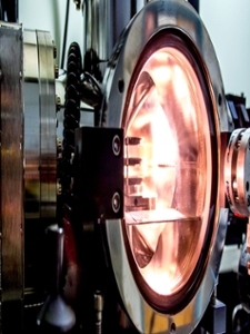
“Using the metal-organic chemical vapor deposition (MOCVD) system and the Nanofabrication Facility at the Center for High Technology Materials, we are studying selective-area regrowth and related doping and defects on nonpolar orientations of GaN, which constitute the regrowth sidewalls when forming p-n junctions in etched trenches,” notes Feezell. "The goal is to enable a fundamental understanding of the regrowth interface that will lead to high-voltage diodes with low leakage current.”
The teams at UNM and Sandia are seeking to achieve selective-area doping using patterned regrowth of GaN p-n diodes with electronic performance equivalent to as-grown, state-of-the-art GaN p-n diodes. They are working to obtain a deep understanding of the growth process, including the relationship among crystal growth conditions, etching methods and post-etch treatments, impurity control, and electronic performance.
Feezell concludes “Our research in this area will generate knowledge needed to address materials challenges for vertical GaN-based power electronic devices and help expedite their adoption in a variety of commercial applications.”
